
Introduction:
Spintronics or spin transport electronics has emerged with a promise that we can now simultaneously use both charge and spin of electrons in a device.
Operation of conventional electronic device such as; transistors, OPAMPs Integrated Circuits (ICs) solely depends on the transport of the charge carriers (electrons/holes) and spin is ignored totally. In contrast, a spintronic device measures the difference in transport of “spin up” and “spin down” electrons in the circuit. During last 30 years the idea of spintronics technology has flourished and has created huge job openings for engineers and scientists. The journey was started following the discovery of giant magneto resistance (GMR) in 1988. At present, GMR based sensors are used in hard drives, in robotics, electric vehicles, MRAMs, Industrial motors, magnetic sensing and in navigation.
What is Spin and how it can be used in a Device??
An electron has 3 fundamental properties; charge (e = -1.602×10⁻¹⁹ C), mass (9.1×10⁻¹⁹ kg) and spin. In addition an electron has two kinds of angular momentum that describes it’s orbital motion and spin motion separately. All particles in our world are classified according to their spins. Some of them have integer spin are called bosons and others have half integer spin called fermions. According to quantum mechanics an electron have spin either (+1/2) or (-1/2).
Motion of electrons inside a conductor is described by electrical current (I) is defined as: I = q/t (in units of Ampere). Spin is another fundamental quantity like charge could be detected by measuring magnetic moment (in units of Bohr magneton  of an electron). All kinds of magnetic ordering and interaction inside a solid are now explained through spin of electrons.
Spin of an electron can have two stable states; “spin up” and “spin down” in presence of magnetic field. The spin up and down states of an electron can be used to represent the two binary logic states: 0 and 1. The idea behind spintronic technology is to encode information in these two spin states.
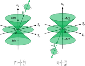
Figure 1: Description of spin angular momentum of spins ½ particles (Reference: Wikipedia.Org).
Importance of Spin electronics …
- Movement of spins like flow of charges can also carry information in a device.
- Spin transport requires less amount of energy than that of charge transport in electronic circuits.
- Once spin state (up or down) is created for an electron it would stay in that state unless we change it by applying field.
- Spin states can be flipped quickly (up to down) and easily by switching the external magnetic field.
Applications: (i) Magnetic sensors (ii) Non-volatile RAM (iii) Quantum computing.
Developments of Spintronic Devices in Laboratory:
The first breakthrough in this field came in 1988, with the discovery of giant magneto resistance (GMR) by Albert Fert in France and Peter Gruenberg in Germany. After that several milestones has been reached and now we can broadly categorized all spin electronic devices into four groups
- Spin valves based on magnetic nonmagnetic layered structure.
- Magnetic tunnel junctions
- Ferromagnetic-semiconductor hybrid structure
- Organic devices
- Spin Valves: A schematic of layered ferromagnetic (FM)/nonmagnetic (NM) “spin valve” structure is represented in Figure 2. Spin orientation in a given layer could be changed by external field.
GMR Device: A thin NM metallic layer is sandwiched between two magnetic layers; presented in Figure 2. The conduction electrons became spin polarised while passing through the FM layer. The resistance is minimum (Rmin) if spins of the neighbouring magnetic layers are aligning parallel. If magnetic layers have opposite spin configuration then resistance is maximum (Rmax) and GRM ratio is defined as 

Figure 2: Schematic of layered FM/NM structure (Source: https://www.physicscentral.com)
- Magnetic tunnel junctions (MTJ): The structure is similar as described above; the only difference is that NM metallic layer is replaced ultra-thin insulating oxide (Al2O3/MgO) layer. Electrons can tunnel through one magnetic layer to other easily when both them have same spin configuration otherwise resistance is high. The spin dependent tunnelling current in MTJs depends on the structure and morphology at the interface with the FM layer. Like GMR, MTJs are used for fabrication of spin valves.
- Ferromagnetic/semiconductor hybrid structure: Different types like; Schottky Diode, Spin FET, Spin LED, Spin transistors belong to this category. There is another type; known as “Diluted magnetic semiconductors” have been studied extensively in last two decades. The idea was to introduce magnetic elements; such as Mn (transition metals: d block element) as dopants in semiconductors such as; GaN, GaAs to produce a magnetic semiconductors. They are fascinating because within a single device we could see amplification of electrical signals in addition spin polarized carriers could be used for storing information.
- Organic Devices: Recently organic materials (grapheme, carbon nanotubes) have been used as NM media to store and carry spin polarized carriers (electrons/holes). A new research field “molecular electronics” has evolved recently which aims to build electronic devices from single molecules.
A Journey from Laboratory to Industry:
Scientist came up with idea, technologist converts it into devices and industry came up with the final product, if it is profitable. The journey began when IBM industry first implemented GMR “spin-valve” into hard drives. This “spin-valve” technology ensures better storage capacity in magnetic hard drives. IBM research scientist, Dr. Stuart Parkin with his colleagues had taken initiatives to commercialize this “spin-valve” technology. The first spin valve sensor “Deskstar 16 GP Titan” (capacity 16.8 GB) released into market in 1997, within 10 years of the discovery of GMR. In September 2007 “The New York times” reports that the huge increase of digital storage capacity by virtue of “spin-valve” technology made possible consumer audio and video iPods, and Google style giant data centres in reality. Latter Hitachi (2013 onwards) had launch model: 7K 1000 with 1 TB capacity and model: 7K 3000 with 3 TB of storage capacity. We could never find such a rapid development in any other scientific field.
Over the last two decades physicist and technologist around the world had work hard on TMR spin valves (MTJs). These MTJs could be used in magnetic random access memory (MRAM) cell, perhaps the best commercially useful spintronic product. Several companies; Everspin-technologies, Freescale, IBM-corporation, Inter-corporation, Hitachi, Micron, and startup groups in collaboration with research institutes are involved now in MRAM technology. The larger storage space and faster data transfer speed of MRAMs make it more useful and it might replace the other memory chips such as; SRAM, DRAM, Flash-memory in future. In addition MRAM is non-volatile means no information is lost when powered off. It consumes less power and is more robust hence suitable for extreme condition to work such as; at high temperature or in high level of radiation.
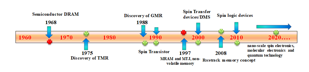
Figure 3: Major breakthroughs in spintronic field. Red cross symbol represents commercialize technology and green cross represents the scientific idea. (Reference: https://doi.org/10.1038/s43246-020-0022-5).
Conclusion and Future Prospect:
Spin-electronics involve active control and manipulation of electron’s spin in solid state devices. However this novel idea could be realized only if the 3 requirements; (i) Efficient spin injection (ii) Slow spin relaxation and (iii) reliable spin detection are satisfied. At present hard drives and MRAMs holds the market for spintronics however it is difficult to predict in which direction it will move in future. Faster data transfer speed with high storage capacity requires nanoscale fabrication of these devices to enhance the areal density in hard drives. But it causes enhancement in energy consumption. It is possible that spintronics successfully used in quantum computation in future. On-going research and development in this field during last 30 years is very promising, so in my opinion it will enhance the job opportunities and may controls the economic growth of several countries.
Visited 2635 times, 2 Visits today